Thermal ALD
In most ALD reactions, two chemicals are used as precursors. These precursors react with the material surface in a continuous and self-limiting manner.
Atomic Layer Deposition System
ALD is for thin film deposition is one of the most important techniques based on the sequential use of a gas phase chemical process; It can be considered as a special type of chemical vapor deposition (CVD). The majority of ALD reactions use two or more chemicals called precursors (also called "reactants"). These precursors react with the surface of a material one at a time in a sequential, self-limiting, manner. Through the number of ALD cycles, a thin film is slowly deposited. ALD is a important process in manufacturing semiconductor devices, and part of the set of tools available for synthesizing nanomaterials.
ALD has a number of advantages such as excellent uniformity, film conformality with identical film thicknesses deposited on the wafer surface even complex shapes substrates, low temperature processing. Therefore, ALD is applied for many applications in the field of microelectronics, nanotechnology and biotechnology which often working on soft substrates, such as organic and biological samples.
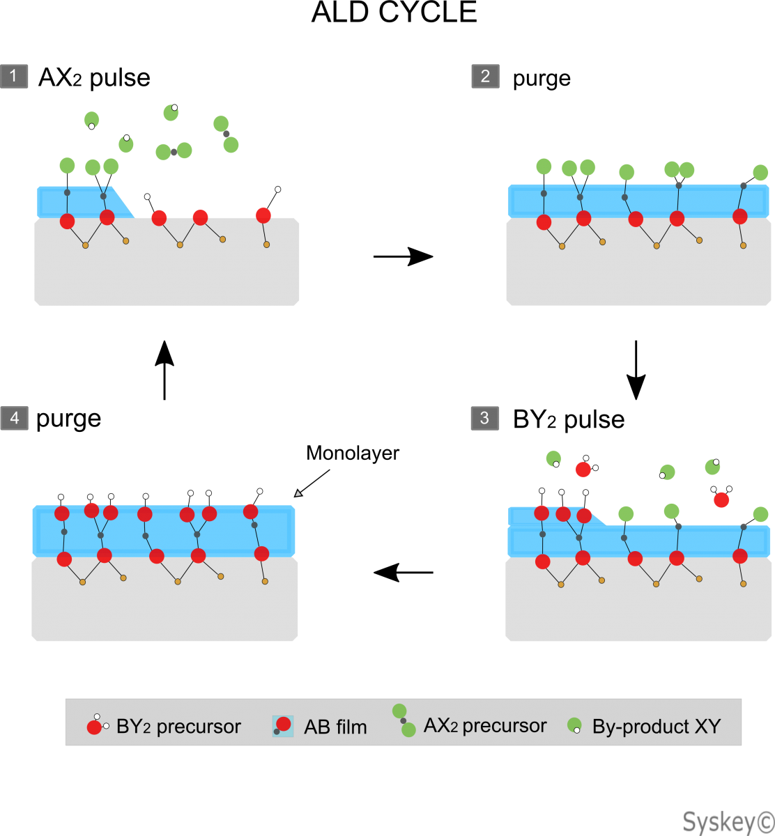
Figure 1: Schematic Diagram-ALD.
Thickness Uniformity (WIW):
A single 12-inch wafer is used to deposit Al2O3 and HfO2 films with a target thickness of 5nm. Use an ellipsometer (ellipsometer) to make a 27-point thickness measurement and bring in the standard deviation formula. Within ± 0.5nm and within 5% of uniformity.
| Al2O3 Uniformity=1.58% |
HlfO2 Uniformity=1.27% |
.png) |
.png) |
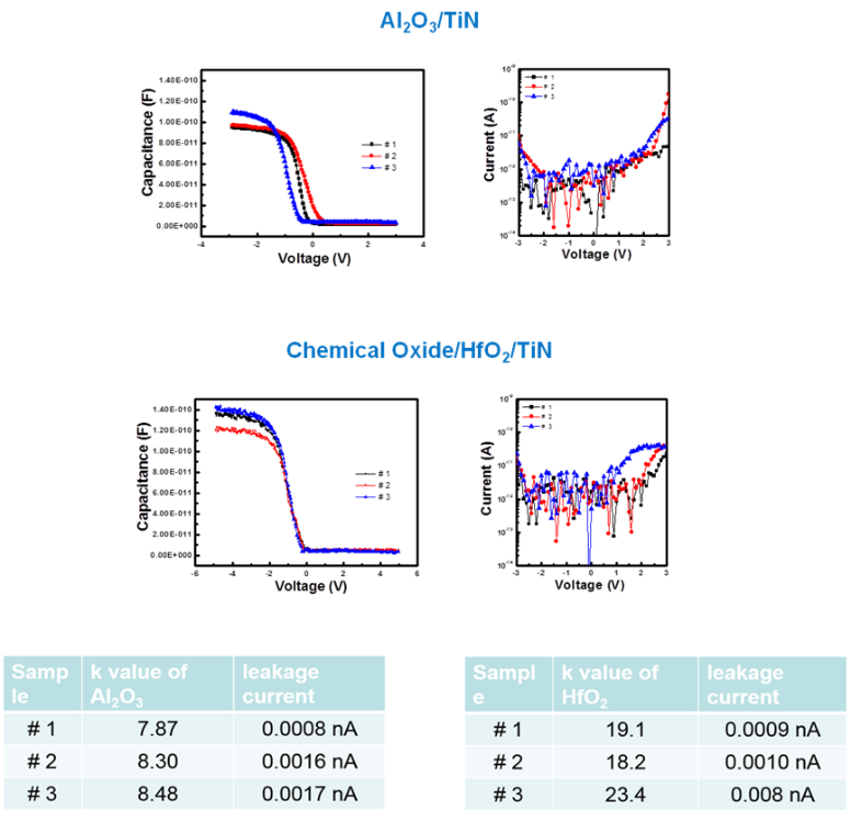
Dielectric constant and work function:
Prepare three silicon wafers and deposit Al2O3/ TiN and chemical oxide / HfO2 / TiN with a fixed thickness. Measure the CV diagrams of the three samples to calculate the dielectric constant and leakage current: The dielectric constant should be 7 ~ 9 (Al2O3) and 18 ~ 22 (HfO2), and the leakage current is less than 1nA (@ 1V).